

The Silicon Revolution in Your Pocket
Every time you unlock your smartphone, send a message, or stream a video, you’re witnessing the magic of semiconductor electronics in action. The tiny chip inside your phone contains billions of semiconducting devices working together at lightning speed. From the LED lights illuminating your room to the solar panels on rooftops, semiconductor materials have revolutionized our world in ways that seemed impossible just decades ago.
Chapter 14 of CBSE Class 12 Physics takes you on this fascinating journey through the world of semiconductors – the materials that bridge the gap between conductors and insulators. You’ll discover how pure silicon transforms into the building blocks of modern technology, how p-n junctions create the foundation for all electronic devices, and how simple combinations of these elements create the complex circuits that power our digital age.
This comprehensive study guide will transform your understanding of semiconductor physics from abstract concepts into practical knowledge that connects directly to the technology around you. Whether you’re aiming for top marks in your board exam or building a foundation for engineering studies, this guide provides everything you need to master semiconductor electronics with confidence.
Learning Objectives: What You’ll Master by Chapter’s End
By completing this chapter, you will demonstrate mastery of:
- Material Properties: Distinguish between intrinsic and extrinsic semiconductors and explain doping mechanisms
- Energy Band Theory: Analyze energy band diagrams and predict electrical behavior of materials
- P-N Junction Physics: Understand junction formation, depletion regions, and forward/reverse biasing
- Diode Applications: Apply diode characteristics to rectification and voltage regulation circuits
- Transistor Operation: Explain bipolar junction transistor functioning and switching behavior
- Amplification Principles: Calculate gain parameters and design basic amplifier circuits
- Logic Gate Implementation: Construct digital circuits using AND, OR, NOT, NAND, and NOR gates
- Circuit Analysis: Solve complex problems involving semiconductor devices in practical circuits
- Experimental Skills: Design investigations to measure semiconductor device characteristics
1: Understanding Semiconductor Materials – The Foundation of Modern Electronics
The Material Spectrum: From Insulators to Superconductors
Imagine materials arranged on a spectrum based on their ability to conduct electricity. At one extreme, you have insulators like rubber and glass, where electrons are tightly bound to atoms and resist movement. At the other extreme lie conductors like copper and silver, where electrons move freely like water flowing through an open pipe.
Semiconductors occupy the fascinating middle ground. Think of them as materials with adjustable electrical properties – like a water faucet that you can turn to control the flow. Pure semiconductors like silicon and germanium have moderate conductivity at room temperature, but here’s where it gets interesting: their electrical properties can be dramatically altered by adding tiny amounts of impurities, a process called doping.
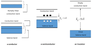
Intrinsic Semiconductors: Pure and Pristine
Pure silicon crystal represents an intrinsic semiconductor in its natural state. At absolute zero temperature, all electrons are bound in covalent bonds, making silicon behave like an insulator. However, as temperature increases, thermal energy breaks some covalent bonds, freeing electrons and creating positively charged holes.
The relationship between temperature and conductivity in intrinsic semiconductors follows:
[EQUATION: σ = σ₀e^(-Eg/2kT)]
Where σ is conductivity, Eg is the energy gap, k is Boltzmann’s constant, and T is absolute temperature.
Physics Check Box:
Why does a semiconductor’s resistance decrease with increasing temperature, while a metal’s resistance increases? In semiconductors, higher temperature creates more charge carriers (electrons and holes), increasing conductivity. In metals, higher temperature causes more atomic vibrations, which scatter electrons and increase resistance.
Extrinsic Semiconductors: Engineering Electrical Properties
The real power of semiconductors emerges when we introduce controlled impurities through doping. This process is like adding a tiny amount of salt to change water’s properties – except here, we’re adding atoms with different valence electrons to alter electrical behavior.
N-Type Doping: Creating Electron Highways
When we add pentavalent atoms (like phosphorus or arsenic) to pure silicon, each impurity atom contributes an extra electron. These donor atoms create n-type semiconductors where electrons are the majority charge carriers. Picture this as adding extra workers to a factory – productivity (conductivity) increases dramatically.
P-Type Doping: Manufacturing Electron Vacancies
Introducing trivalent atoms (like boron or aluminum) creates electron-deficient regions called holes. These acceptor atoms produce p-type semiconductors where holes act as majority carriers. Think of holes as job openings that electrons can fill, creating apparent positive charge movement.
Real-World Physics Box:
Modern computer processors contain billions of p-type and n-type regions etched onto silicon wafers thinner than human hair. Each transistor switches billions of times per second, with doping concentrations precise to parts per billion – more precise than mixing one teaspoon of sugar into an Olympic-sized swimming pool!
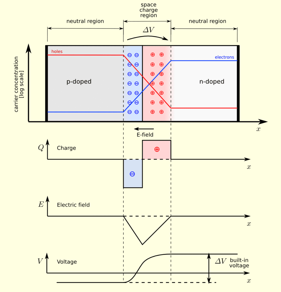
2: The P-N Junction – Where Magic Happens
Junction Formation: When Opposites Attract
When p-type and n-type semiconductors are joined, nature performs an elegant balancing act. Electrons from the n-side diffuse toward the p-side, while holes migrate in the opposite direction. This movement creates a depletion region – a zone depleted of mobile charge carriers but rich in fixed ionized atoms.
The process resembles two crowds meeting at a doorway – initial mixing occurs, but eventually, a barrier forms that prevents further movement. This barrier, called the built-in potential (V₀), typically measures about 0.7V for silicon junctions.
[EQUATION: V₀ = (kT/e) × ln(Na×Nd/ni²)]
Where Na and Nd are acceptor and donor concentrations, and ni is the intrinsic carrier concentration.
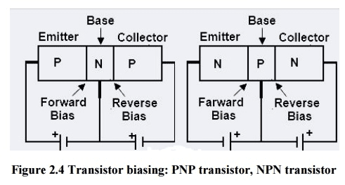
Forward Bias: Opening the Electronic Gateway
When we apply external voltage with the positive terminal connected to the p-side and negative to the n-side, we create forward bias conditions. This external voltage opposes the built-in potential, reducing the barrier height and allowing current to flow.
Forward bias operation resembles opening flood gates – once the external voltage exceeds the built-in potential (approximately 0.7V for silicon), current increases exponentially according to the diode equation:
[EQUATION: I = Is(e^(V/ηVT) – 1)]
Where Is is the saturation current, V is the applied voltage, η is the ideality factor, and VT is the thermal voltage.
Reverse Bias: The Electronic One-Way Street
Applying voltage in the opposite direction (positive to n-side, negative to p-side) creates reverse bias. This configuration widens the depletion region and increases the potential barrier, effectively blocking current flow. Only a tiny reverse saturation current flows, making the p-n junction behave like an electronic one-way street.
Common Error Alert:
Students often confuse forward and reverse bias directions. Remember: Forward bias = p-side positive, n-side negative. Think “positive to p” for forward conduction.
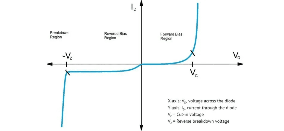
3: Diodes in Action – From Concept to Circuit
The Diode I-V Characteristic: Understanding the Electronic Personality
Every diode has a unique personality described by its current-voltage (I-V) characteristic curve. In forward bias, current remains negligible until the applied voltage exceeds the threshold voltage (≈0.7V for silicon). Beyond this point, current increases exponentially – small voltage increases produce dramatic current changes.
In reverse bias, current remains constant at the tiny reverse saturation value until the reverse voltage becomes large enough to cause breakdown. This behavior makes diodes perfect for one-way current flow applications.
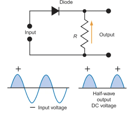
Rectification: Converting AC to DC Power
One of the most practical applications of diodes involves converting alternating current (AC) from power outlets into direct current (DC) needed by electronic devices. Your laptop charger, phone adapter, and LED bulb drivers all use diode rectification circuits.
Half-Wave Rectification: Simple but Inefficient
In half-wave rectification, a single diode allows only positive (or negative) half-cycles of AC voltage to pass through. While simple, this wastes half the available power and produces significant ripple in the output.
[EQUATION: Efficiency = (Power delivered to load)/(AC input power) = 40.6%]
Full-Wave Rectification: Maximizing Power Transfer
Full-wave rectifiers use multiple diodes to utilize both positive and negative half-cycles, doubling efficiency and reducing ripple. Center-tap and bridge configurations represent the two main approaches.
Problem-Solving Strategy Box:
When analyzing rectifier circuits:
- Identify which diodes conduct during each half-cycle
- Trace current path through conducting diodes
- Calculate output voltage considering diode voltage drops
- Determine ripple factor and efficiency
- Consider filter capacitor effects on output smoothing
Voltage Regulation: Zener Diodes as Electronic Governors
Zener diodes operate in the reverse breakdown region to provide constant voltage output despite varying input voltage or load current. They function like electronic pressure regulators, maintaining steady voltage just as a pressure regulator maintains constant water pressure.
The Zener voltage remains essentially constant over a wide current range, making these devices invaluable for creating stable voltage references in power supplies and measurement circuits.
[EQUATION: Voltage regulation = (VNL – VFL)/VFL × 100%]
Where VNL is no-load voltage and VFL is full-load voltage.
4: Bipolar Junction Transistors – The Workhorses of Electronics
Transistor Structure: Three Layers of Semiconductor Magic
A bipolar junction transistor (BJT) consists of three alternating semiconductor regions: emitter, base, and collector. Think of it as two back-to-back p-n junctions sharing a common middle region. The arrangement can be either n-p-n or p-n-p, creating complementary devices with opposite polarities.
The key to transistor operation lies in the base region’s extreme thinness – typically less than 1 micrometer wide. This narrow base allows most charge carriers injected from the emitter to traverse to the collector without recombining, enabling current amplification.
Current Amplification: Small Input, Big Output
The transistor’s magic lies in its ability to control large collector current with small base current changes. This current amplification occurs because the emitter injects many charge carriers into the thin base region, and most of these carriers reach the collector.
The current gain (β or hfe) quantifies this amplification:
[EQUATION: β = IC/IB = ΔIC/ΔIB]
Typical β values range from 50 to 500, meaning a 1 mA change in base current can control a 100-500 mA change in collector current.
Real-World Physics Box:
The first transistor, invented at Bell Labs in 1947, was barely functional and used germanium crystals with gold point contacts. Today’s smartphone processors contain over 10 billion transistors, each smaller than a virus, switching trillions of times per second while consuming less power than a small LED!
Common Emitter Configuration: The Versatile Amplifier
The common emitter (CE) configuration provides both current and voltage amplification, making it the most popular transistor amplifier arrangement. In CE mode, the input signal applies between base and emitter, while output appears between collector and emitter.
Key CE parameters include:
- Current gain: β = IC/IB
- Voltage gain: Av = -β × (RC/re), where re is dynamic emitter resistance
- Input resistance: Rin ≈ β × re
- Output resistance: Rout ≈ RC
[EQUATION: re = VT/IE ≈ 26mV/IE at room temperature]
Physics Check Box:
Why is the voltage gain negative in common emitter amplifiers? When base current increases, collector current increases, causing larger voltage drop across the collector resistor. This reduces collector voltage relative to ground, creating 180° phase inversion between input and output signals.
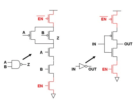
Transistor as a Switch: Digital Logic Foundation
In switching applications, transistors operate in either cut-off (OFF) or saturation (ON) modes, avoiding the linear amplification region. This binary operation forms the basis for all digital logic and computer processing.
Cut-off Mode: No base current flows, resulting in zero collector current. The transistor acts like an open switch.
Saturation Mode: Base current is sufficient to drive the collector to its maximum current, limited by external circuit resistance. The transistor acts like a closed switch with minimal voltage drop.
The switching speed depends on charge storage and transit times, with modern transistors switching in picoseconds – fast enough to enable gigahertz processor speeds.
5: Digital Logic Gates – Building Blocks of the Information Age
Boolean Logic in Silicon: From Math to Reality
Digital logic gates implement Boolean algebra using transistor switches, transforming abstract mathematical concepts into physical reality. Each gate performs a specific logical operation on binary inputs (0s and 1s), producing predictable binary outputs.
The beauty of digital systems lies in their noise immunity – signals need only distinguish between two states rather than preserving exact analog values. This robustness enables error-free information processing across billions of operations.
Fundamental Logic Gates: The Digital Toolkit
NOT Gate (Inverter): The Digital Opposer
The NOT gate produces an output opposite to its input – if input is HIGH (1), output is LOW (0), and vice versa. Transistor implementation uses the switching principle: when input voltage is high enough to saturate the transistor, output drops to near zero volts.
Truth Table for NOT Gate:
Input (A) | Output (Y)
    0     |     1
    1     |     0
AND Gate: Digital Multiplication
An AND gate outputs HIGH only when ALL inputs are HIGH. Think of it as a series circuit where all switches must be closed for current to flow. The Boolean expression is Y = A · B for a two-input AND gate.
OR Gate: Digital Addition
An OR gate outputs HIGH when ANY input is HIGH. This resembles a parallel circuit where closing any switch allows current to flow. The Boolean expression is Y = A + B for a two-input OR gate.
Universal Gates: NAND and NOR Supremacy
NAND Gate: The Universal Building Block
NAND (NOT-AND) gates are called universal because any Boolean function can be implemented using only NAND gates. This universality makes NAND gates the preferred choice for integrated circuit design, simplifying manufacturing and reducing costs.
The NAND gate’s versatility stems from its ability to implement all other gates:
- NOT gate: Connect both NAND inputs together
- AND gate: NAND followed by NOT (another NAND with inputs tied)
- OR gate: Use De Morgan’s theorem with NAND gates
Problem-Solving Strategy Box:
When designing logic circuits:
- Write the Boolean expression for desired function
- Identify required gates from truth table analysis
- Minimize expression using Boolean algebra or K-maps
- Convert to available gate types (often NAND-only)
- Verify operation with test inputs
- Consider propagation delays in timing analysis
Combinational vs Sequential Logic: Static vs Dynamic Behavior
Combinational Logic: Outputs depend only on current inputs. Examples include adders, multiplexers, and decoders. Response is instantaneous (limited only by propagation delays).
Sequential Logic: Outputs depend on both current inputs and previous states, requiring memory elements like flip-flops. Examples include counters, registers, and state machines.
Modern computers use both types – combinational logic for arithmetic and data processing, sequential logic for memory and control functions.
Real-World Physics Box:
A modern CPU contains billions of logic gates switching at frequencies exceeding 3 GHz. At these speeds, the time for light to travel one centimeter (about 33 picoseconds) becomes significant compared to gate switching times. This is why computer engineers must consider relativistic effects in high-speed digital design!
6: Advanced Applications and Integration
Operational Amplifiers: Analog Signal Processing
While this chapter focuses on digital applications, understanding how transistors enable analog signal processing provides crucial insight into complete electronic systems. Operational amplifiers (op-amps) use multiple transistor stages to achieve extremely high gain and precise signal manipulation.
Op-amp applications include:
- Signal amplification with programmable gain
- Mathematical operations (addition, subtraction, integration)
- Active filters for frequency-selective circuits
- Voltage followers for impedance matching
- Comparators for analog-to-digital conversion
Integrated Circuits: Miniaturization Revolution
The transition from individual transistors to integrated circuits (ICs) revolutionized electronics by enabling complex systems on tiny silicon chips. Moore’s Law – the observation that transistor density doubles every two years – has driven continuous miniaturization for over five decades.
Modern IC fabrication involves:
- Photolithography for precise pattern transfer
- Ion implantation for controlled doping
- Chemical vapor deposition for layer formation
- Etching processes for material removal
- Multiple metallization layers for interconnection
Power Electronics: High-Current Applications
While logic circuits handle information, power electronics control energy flow in applications ranging from LED drivers to electric vehicle motor controllers. Power semiconductors operate at higher voltages and currents, requiring careful thermal management and protection circuits.
Key power devices include:
- Power MOSFETs for switching applications
- IGBTs (Insulated Gate Bipolar Transistors) for high-power control
- Power diodes for rectification and protection
- Thyristors for AC power control
7: Laboratory Investigations and Practical Skills
Measuring Diode Characteristics: Hands-On Discovery
Experiment 1: Forward and Reverse Bias Investigation
Objective: Determine the I-V characteristic of a silicon diode and verify theoretical predictions.
Procedure:
- Connect diode in forward bias with variable DC supply and ammeter/voltmeter
- Gradually increase applied voltage from 0 to 1.0V in 0.1V steps
- Record current and voltage at each step
- Repeat in reverse bias up to maximum safe reverse voltage
- Plot I-V characteristic curve and identify key parameters
Expected Results:
- Forward threshold voltage ≈ 0.7V for silicon diodes
- Exponential current increase beyond threshold
- Constant reverse saturation current in reverse bias
- Sharp breakdown at reverse breakdown voltage
Data Analysis Techniques:
- Use semi-logarithmic plots to verify exponential relationship
- Calculate ideality factor from slope analysis
- Determine reverse saturation current from reverse bias data
- Estimate breakdown voltage from reverse characteristic
Transistor Testing: Verifying Amplification
Experiment 2: Common Emitter Amplifier Characteristics
This investigation demonstrates current amplification and voltage gain in the versatile CE configuration.
Key Measurements:
- Input characteristics: IB vs VBE for constant VCE
- Output characteristics: IC vs VCE for constant IB
- Transfer characteristics: IC vs IB for constant VCE
- Frequency response: gain vs frequency
Error Analysis Considerations:
- Temperature effects on semiconductor parameters
- Loading effects of measurement instruments
- Parasitic capacitances affecting high-frequency response
- Non-linearities at extreme operating points
Common Error Alert:
When measuring transistor characteristics, always limit maximum power dissipation to prevent thermal damage. Calculate power as P = VCE × IC and stay below device ratings (typically 1-2 watts for small signal transistors).
Logic Gate Verification: Digital Truth Tables
Experiment 3: Logic Gate Implementation and Testing
Using discrete transistors or IC logic gates, verify truth table operations for fundamental gates.
Testing Procedure:
- Apply all possible input combinations
- Measure output voltages for each combination
- Verify HIGH/LOW voltage levels meet specifications
- Measure propagation delays with oscilloscope
- Test fan-out capabilities with multiple loads
Practice Problems Section: Mastering Semiconductor Calculations
Problem Set 1: Intrinsic and Extrinsic Semiconductors
Problem 1.1 (Multiple Choice):
The conductivity of an intrinsic semiconductor at 300K is 10⁻⁶ S/m. If the energy gap is 1.1 eV, what is the approximate conductivity at 350K?
A) 5.7 × 10⁻⁶ S/m
B) 1.2 × 10⁻⁵ S/m
C) 2.8 × 10⁻⁵ S/m
D) 4.5 × 10⁻⁵ S/m
Solution:
Using σ = σ₀e^(-Eg/2kT):
σ₃₅₀/σ₃₀₀ = exp[-Eg/2k × (1/350 – 1/300)]
= exp[-1.1 × 1.6×10⁻¹⁹/(2 × 1.38×10⁻²³) × (-4.76×10⁻⁴)]
= exp[2.87] ≈ 17.6
σ₃₅₀ = 17.6 × 10⁻⁶ = 1.76 × 10⁻⁵ S/m
Answer: B) 1.2 × 10⁻⁵ S/m (closest value)
Problem 1.2 (Free Response):
Calculate the hole concentration in p-type silicon doped with 10¹⁶ boron atoms/cm³ at room temperature. Given: ni = 1.5 × 10¹⁰ cm⁻³.
Solution:
For p-type semiconductor: p ≈ Na (assuming complete ionization)
p = 10¹⁶ cm⁻³
Using mass action law: n × p = ni²
n = ni²/p = (1.5 × 10¹⁰)²/10¹⁶ = 2.25 × 10⁴ cm⁻³
Therefore: p = 10¹⁶ cm⁻³, n = 2.25 × 10⁴ cm⁻³
Problem Set 2: P-N Junction and Diode Applications
Problem 2.1 (Circuit Analysis):
In the circuit shown, determine the current through the 1kΩ resistor when the input voltage is +5V. Assume the diode has a 0.7V forward voltage drop and is ideal otherwise.
[Circuit: 5V source → 1kΩ resistor → silicon diode → ground]
Solution:
Since input voltage (5V) exceeds diode threshold (0.7V), the diode conducts.
Voltage across resistor = 5V – 0.7V = 4.3V
Current = V/R = 4.3V/1000Ω = 4.3 mA
Problem 2.2 (Rectifier Design):
Design a full-wave bridge rectifier to convert 120V RMS AC to approximately 15V DC with less than 5% ripple. Calculate required transformer ratio and filter capacitor value.
Solution:
For bridge rectifier: Vpeak = √2 × Vrms = √2 × 120V = 170V
Required transformer secondary: Vs = 15V × √2 = 21.2V RMS
Transformer ratio = 120V/21.2V = 5.66:1
For 5% ripple with 60Hz full-wave (120Hz ripple):
Ripple factor = 1/(4√3 × f × R × C) ≤ 0.05
Assuming R = 1kΩ: C ≥ 1/(4√3 × 120 × 1000 × 0.05) = 2400 μF
Use 2500 μF capacitor for safety margin.
Problem Set 3: Transistor Amplifiers and Switching
Problem 3.1 (Amplifier Analysis):
A common emitter amplifier has the following parameters: β = 100, VCC = 12V, RC = 2kΩ, RE = 1kΩ, R1 = 10kΩ, R2 = 2kΩ. Calculate the voltage gain and input resistance.
Solution:
First, find the Q-point (operating point):
VB = VCC × R2/(R1 + R2) = 12V × 2kΩ/12kΩ = 2V
VE = VB – VBE = 2V – 0.7V = 1.3V
IE = VE/RE = 1.3V/1kΩ = 1.3 mA
IC ≈ IE = 1.3 mA (since β >> 1)
Dynamic emitter resistance: re = 26mV/IE = 26mV/1.3mA = 20Ω
Voltage gain: Av = -RC/re = -2000Ω/20Ω = -100
Input resistance: Rin = β × re = 100 × 20Ω = 2kΩ
Problem 3.2 (Switching Application):
Design a transistor switch to control a 12V, 100mA LED load using a 5V logic signal. Select appropriate base resistor value assuming β = 50.
Solution:
For saturation: IC(sat) = 100mA (LED current)
Required base current: IB = IC/β = 100mA/50 = 2mA
Use IB = 5mA for reliable saturation (2.5× overdrive)
Base resistor: RB = (VLogic – VBE)/IB = (5V – 0.7V)/5mA = 860Ω
Use standard 820Ω resistor.
Problem Set 4: Logic Gates and Digital Circuits
Problem 4.1 (Boolean Algebra):
Simplify the Boolean expression: F = A̅B̅C + A̅BC̅ + AB̅C̅ + ABC
Solution:
F = A̅B̅C + A̅BC̅ + AB̅C̅ + ABC
Group terms: F = A̅C(B̅ + B) + AB̅C̅ + ABC
Since (B̅ + B) = 1: F = A̅C + AB̅C̅ + ABC
Factor AC terms: F = A̅C + A(B̅C̅ + BC)
Further simplification: F = A̅C + A(B ⊕ C)̅
Final form: F = A̅C + A(B̅C̅ + BC)
Problem 4.2 (Circuit Design):
Implement the function F = (A + B)(C + D) using only NAND gates.
Solution:
Using De Morgan’s theorems:
F = (A + B)(C + D)
Apply De Morgan’s: F = ((A + B)̅)̅ · ((C + D)̅)̅
= (A̅B̅)̅ · (C̅D̅)̅
= ((A̅B̅) + (C̅D̅))̅ [De Morgan’s again]
= (A̅B̅ + C̅D̅)̅
This can be implemented with:
- NAND gate 1: inputs A, A → A̅
- NAND gate 2: inputs B, B → B̅
- NAND gate 3: inputs A̅, B̅ → A̅B̅
- Similar for C̅D̅
- Final NAND gate combines the results
Problem Set 5: Comprehensive Applications
Problem 5.1 (Multi-Stage Analysis):
A two-stage amplifier uses identical CE stages, each with voltage gain of -50. If the input signal is 10mV RMS, calculate the output voltage and overall gain.
Solution:
Stage 1 output = -50 × 10mV = -500mV
Stage 2 output = -50 × (-500mV) = +25V RMS
Overall gain = Av1 × Av2 = (-50) × (-50) = +2500
Verification: 2500 × 10mV = 25V ✓
Problem 5.2 (Power Supply Design):
Design a complete power supply to convert 230V AC to regulated +5V DC capable of supplying 2A load current. Include rectification, filtering, and regulation stages.
Solution:
Transformer: 230V primary to 12V secondary (safety margin for regulation)
Bridge rectifier: 4 × 1N4007 diodes (1000V PIV, 1A rating)
Filter capacitor: For 1% ripple at 2A load:
C = I/(2 × f × ΔV) = 2A/(2 × 50Hz × 0.05V) = 400mF
Voltage regulator: 7805 IC (5V, 1.5A max) or multiple parallel regulators
Heat sink calculation: Power dissipated = (Vin – Vout) × Iout = 7V × 2A = 14W
Required thermal resistance ≤ (125°C – 50°C)/14W = 5.4°C/W
Exam Preparation Strategies: Maximizing Your Board Performance
Understanding Question Patterns: CBSE Board Trends
Weightage Distribution:
- Semiconductor materials and doping: 15% (2-3 marks)
- P-N junction and diode applications: 25% (4-5 marks)
- Transistor characteristics and amplifiers: 35% (6-7 marks)
- Logic gates and digital circuits: 20% (3-4 marks)
- Numerical problems and applications: 5% (1-2 marks)
Common Question Types:
- Conceptual Questions (1-2 marks): Define terms, explain phenomena, state applications
- Diagram-Based Questions (2-3 marks): Draw and label circuits, energy bands, characteristics
- Analytical Questions (3-5 marks): Derive expressions, explain working principles
- Numerical Problems (2-4 marks): Calculate gain, current, voltage, design parameters
- Application Questions (3-5 marks): Real-world problem solving, circuit analysis
Formula Sheet: Essential Equations for Quick Reference
Semiconductor Physics:
- Intrinsic carrier concentration: ni² = np (mass action law)
- Conductivity: σ = e(nμn + pμp)
- Temperature dependence: ni ∝ T^(3/2) × e^(-Eg/2kT)
P-N Junction:
- Built-in potential: V₀ = (kT/e) × ln(NaNd/ni²)
- Depletion width: W = √(2εs(Na+Nd)V₀/eNaNd)
- Diode equation: I = Is(e^(V/ηVT) – 1)
Transistor Parameters:
- Current gain: β = IC/IB, α = IC/IE = β/(β+1)
- Voltage gain (CE): Av = -β(RC/re), where re = VT/IE
- Input resistance: Rin = β × re
- Power gain: Ap = β × Av
Digital Logic:
- De Morgan’s Laws: (A·B)̅ = A̅ + B̅, (A+B)̅ = A̅·B̅
- Boolean identities: A + A̅ = 1, A·A̅ = 0, A + 1 = 1, A·0 = 0
Common Mistakes and Prevention Strategies
Mistake 1: Confusing Forward and Reverse Bias
Prevention: Always remember “Positive to P” for forward bias. Draw clear diagrams showing battery polarity and current direction.
Mistake 2: Incorrect Current Relationships in Transistors
Prevention: Use Kirchhoff’s Current Law at transistor nodes: IE = IC + IB. Remember IC ≈ IE for high β transistors.
Mistake 3: Sign Errors in Amplifier Gain Calculations
Prevention: CE amplifiers always provide 180° phase shift (negative gain). CB and CC configurations have positive voltage gains.
Mistake 4: Boolean Algebra Simplification Errors
Prevention: Work step-by-step, verify each step with truth tables. Use De Morgan’s laws systematically rather than trying shortcuts.
Mistake 5: Units and Significant Figures in Numerical Problems
Prevention: Always check unit consistency. Carry extra significant figures during calculations, round only in final answer.
Conclusion and Next Steps: Building Your Electronics Future
Mastering Chapter 14 – Semiconductor Electronics represents far more than earning marks on your CBSE board exam. You’ve now developed fundamental understanding of the physical principles that power our modern technological civilization. From the smartphone in your pocket to the satellites orbiting Earth, semiconductor devices enable the digital revolution that continues reshaping human society.
Your journey through semiconductor materials, p-n junctions, transistor amplifiers, and digital logic gates provides the essential foundation for advanced studies in electronics engineering, computer science, and applied physics. The problem-solving skills you’ve developed – systematic analysis, mathematical modeling, and experimental verification – transfer directly to university-level coursework and professional engineering practice.
Immediate Next Steps for Board Success:
Focus your remaining preparation time on active problem-solving rather than passive reading. Work through previous year question papers under timed conditions, emphasizing clear diagram drawing and complete numerical solutions. Practice explaining concepts aloud to solidify your understanding and identify any remaining weak areas.
Future Learning Pathways:
Consider exploring advanced topics that build on this foundation: microprocessor architecture, VLSI design, power electronics, or embedded systems programming. Many universities offer excellent resources for self-directed learning in these areas, and practical projects using Arduino or Raspberry Pi platforms provide hands-on experience with the concepts you’ve mastered.
Real-World Connection Opportunities:
Look for internships or project opportunities in electronics companies, research laboratories, or technology startups in your area. Even brief exposure to professional engineering environments will deepen your appreciation for how theoretical knowledge translates into practical innovation.
Historical Context and Future Directions:
The semiconductor revolution that began in the 1940s continues accelerating today. Emerging technologies like quantum computing, neuromorphic processors, and molecular electronics promise to extend the principles you’ve learned into entirely new realms of possibility. Your solid grounding in semiconductor physics positions you to understand and potentially contribute to these exciting developments.
Final Encouragement:
Physics at the Class 12 level represents genuine scientific understanding, not simplified approximations. The equations you’ve learned, the circuits you’ve analyzed, and the principles you’ve mastered are the same tools used by practicing engineers and researchers worldwide. Take pride in joining this global community of scientific thinkers and technological innovators.
Remember that true understanding develops gradually through practice and application. Continue asking questions, making connections between concepts, and seeking opportunities to apply your knowledge creatively. The semiconductor electronics foundation you’ve built will serve you well throughout your academic and professional journey, regardless of which specific career path you ultimately choose.
Your success in mastering this challenging material demonstrates the analytical thinking, mathematical skills, and scientific reasoning that employers and universities highly value. Use this achievement as motivation to continue pushing the boundaries of your scientific understanding, always remembering that today’s impossibilities often become tomorrow’s technological realities through the dedicated efforts of well-prepared students like yourself.
The future of technology depends on the next generation of scientists and engineers who understand both the fundamental principles and practical applications of semiconductor electronics. You are now well-equipped to be part of that future.
This comprehensive study guide provides complete coverage of CBSE Class 12 Physics Chapter 14 – Semiconductor Electronics: Materials, Devices, and Simple Circuits. It includes theoretical concepts, practical applications, solved problems, experimental procedures, and exam strategies designed to ensure thorough understanding and board exam success.
Recommended –